Nanoscale Structures
Nanoscale high aspect ratio structures have possible applications in microfluidic channels, batteries, and fuel cells, among others. We present methods to create 3:1 aspect ratio structures in transparent materials that will withstand temperatures needed for CVD or ALD processes; including contact molding, spin and etch back, and replica molding.
Dielectrophoresis
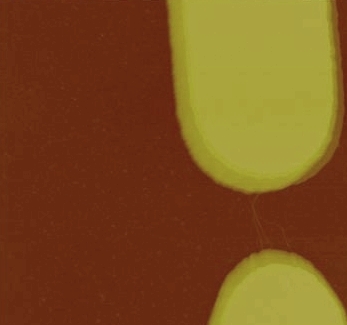
One of the barriers to carbon nanotube electrical device fabrication is the difficulty in controllably placing the nanotubes in the correct positions to form a circuit. Laboratories have found methods to place individual nanotubes, but these methods take hours of man power for each nanotube placement, and are thus suitable only for research and are not scalable. To begin overcoming this barrier, we have sucessfully developed a parallel dielectrophoresis method that allows the precision placement of many nanotubes concurrently in an automated fashion. This is one route that could allow advancements in the field of carbon nanotube electronics.
CNT Microfabrication
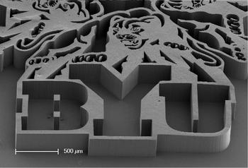
We have developed a surprisingly diverse microfabrication technique that uses carbon nanotubes as scaffolding. The power of this method is that devices with extremely high aspect ratios can be created from out of many different materials using the same base process to define the geometry. Many materials prove nearly impossible to use as the basis of a reasonable structure, because internal stresses build within them as they are deposited. These stresses tend to get stronger and stronger as the material gets thicker. By using carbon nanotubes as the basis of a device, the material of interest needs only to be deposited to a thickness of approximately half the spacing between the nanotubes (on the order of 100 nm) to form a nearly solid device. The carbon nanotubes are a small fraction of the final volume, and can even be removed in some cases. This microfabrication method opens doors to the use of materials that have previously been excluded from the MEMS world, as well as providing countless other design options such as control over porosity, aspect ratio, and other properties.
CNT Purification
The single-walled carbon nanotube is a promising medium in the field of nanoelectronics. However, even the most advanced production methods yield aggregates of both metallic and semiconducting species. If carbon nanotubes are to be used in electrical applications, it is essential that they be isolated according to their electrical conductivity. We are using isopycnic centrifugation to isolate nanotubes. Absorption spectroscopy is used to identify nanotube species within a given sample before and after purification. Our current challenge is to quantify the purity of the isolated semiconducting nanotubes by way of direct measurement. Dielectrophoresis is used to align nanotubes upon electrodes after which individual electrical measurements can be performed. By performing direct measurements on a large sample size of purified semiconducting nanotubes, the effectiveness of this purification technique can be verified electrically.
CNT MEMS
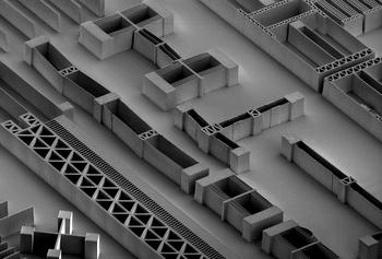
A new approach to the fabrication of microelectronic mechanical devices (MEMS) is a bottom-up design using carbon nanotubes (CNTs). A substrate, typically silicon, is prepared for MEMS construction by first depositing a sacrificial layer of SiO2 for release. Then a 30nm layer of Al2O3 is deposited as a diffusion barrier for the CNT catalyst material (Fe). Next, using photolithography, resist is patterned and developed. A thin layer (4nm) of Fe is deposited on top of the resist and in the trenches where the resist was removed during development. Finally, "lift-off," or removal of the remaining resist, leaves the surface with Fe patterned where CNTs are to be grown. CNTs are grown to various heights, providing high aspect ratios and well-defined features. The CNT "forests" can then be filled with various materials, of which we have tested and operated silicon and silicon nitride devices. To release MEMS devices for operation, the substrate is immersed in HF, removing part of the SiO2 layer below. The new composite's properties were analyzed and compared to MEMS devices fabricated using conventional methods.
Chemical Surface Paterning
Chemical surface patterning at the nanoscale is a critical component of chemically directed assembly of nanoscale devices or sensitive biological molecules onto surfaces. Here we present a scanning probe lithography technique that allows for patterning of aqueous polymers on glass or silicon dioxide surfaces. The surfaces were functionalized by covalently bonding a silane monolayer with a known surface charge to either a glass slide or a silicon wafer. A polymer layer less then 2 nm in thickness was electrostatically bound to the silane layer, passivating the functionalized surface. An Atomic Force Microscope (AFM) probe was used to remove a portion of the polymer layer, exposing the functional silane layer underneath. Employing this method we made chemically active submicron regions. These regions were backfilled with a fluorescent polymer and Lambda-DNA. Chemical differentiation was verified through tapping mode AFM and optical fluorescent microscopy. Lines with a pitch as small as 20nm were observed with AFM height and phase mode data.
Interstitial Filling
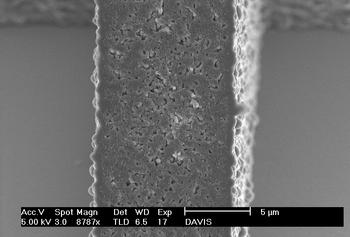 The nanotubes by themselves are not bound together and thus do not form a durable structure, but they can be coated in other materials through various processes such as Chemical Vapor Deposition (CVD) or Electroplating. This has huge advantages because many materials cannot be deposited to high thicknesses without developing too much stress and tearing themselves apart, but when coating carbon nanotubes the filler material need only be deposited to a thickness of a few hundred nanometers in order to form a solid structure of nearly any desired size. This technique also means that high aspect ratio (tall and skinny) devices can be formed from a wide variety of materials, where traditional micromachining is very limited in possible substances and an entirely new process has to be developed to shape each material. Using a carbon nanotube scaffold allows the structure of the device to be predeterminded by one procedure while the material of the device can be determined separately.
Nanoparticles
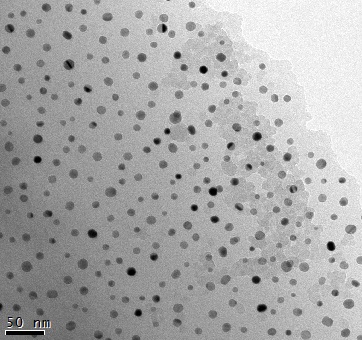
Many metal alloys can form in chemically ordered structures, often resulting in significant changes in properties. The ordered structures are preferred at low temperatures and will go through an order-disorder phase transition at a critical temperature. The formation and stability of these ordered structures in alloy nanoparticles is not well understood but may give insight into the role size plays in phase transitions.
To this end we are studying CoPt, AuCu, and FeNiPt alloy nanoparticles. We characterize these nanoparticles in a Transmission Electron Microscope (TEM) for composition, size, and structure. These nanoparticles are made by co-sputtering the constituents and annealing at different temperatures in various gas mixtures. The nanoparticle samples are prepared for TEM viewing by wedge polishing.