Selected Publications

Thumbnail of figure from publication
By Jorj I. Owen, Travis L. Niederhauser, Brent A. Wacaser, Marc P. Christenson, Robert C. Davis, and Matthew R. Linford
Abstract: This paper describes three advances in lab on a chip technology. First, it is shown that chemomechanical surface patterning can be performed using a commercially available liquid handler that has undergone only minor modifications. These capabilities are demonstrated by making and then characterizing smaller hydrophobic corrals, made with a diamond tip, than have previously been reported. Hydrophobic corrals are small enclosures on a surface that are ringed by hydrophobic lines. They hold droplets of high surface tension solutions. They allow a surface to be subdivided into individually addressable elements, thus providing a platform for conducting many simultaneous surface experiments with small (down to ca. 1 muL) liquid volumes. An important consequence of this work is that it makes chemomechanical surface patterning, which is a valuable and straightforward method for surface modification, much more accessible to the technical community. Second, it is shown that an entire array of hydrophobic corrals can be simultaneously coated with polyelectrolyte multilayers, but that the hydrophobic corrals still retain the ability to hold liquids after this deposition. The robotic arm of the liquid handler is again employed to manufacture this ultrathin film. Finally, as a demonstration of the capability of this technology to create complex patterned arrays on surfaces from solution for biological or nanostructured materials applications, and again employing the liquid handler, polyelectrolyte-coated hydrophobic corrals are individually addressed and loaded with a solution containing gold nanoparticles for independently specified times. The density and morphology of deposited nanoparticle monolayers were studied by scanning electron microscopy. The deposition of gold nanoparticles onto a chip occurred at a constant rate (0.5% min(-1)) over the range of times studied.
Thumbnail of figure from publication
By Jed D. Whittaker, Ghaleb A. Husseini, Matthew R. Linford, and Robert C. Davis (et al.)
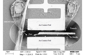
Abstract: A self-aligned thin-film deposition technique was developed to mechanically attach carbon nanotubes to surfaces for the fabrication of structurally robust nanotube-based nanomechanical devices. Single-walled carbon nanotubes were grown by thermal chemical-vapor deposition (CVD) across 150-nm-wide SiO2 trenches. The nanotubes were mechanically attached to the trench tops by selective silicon tetraacetate-based SiO2 CVD. No film was deposited on the nanotubes where they were suspended across the trenches. (C) 2003 American Institute of Physics.
Thumbnail of figure from publication
By Yit-Yian Lua, Travis L. Niederhauser, Brent A. Wacaser, Adam T. Woolley, Robert C. Davis, and Matthew R. Linford (et al.)
Abstract: We recently reported that monolayers on silicon are formed, and silicon surfaces concomitantly patterned, when native oxide-coated silicon is scribed with a diamond-tipped instrument in the presence of reactive liquids. Notably, monolayers were prepared (and are prepared in this work) in an open laboratory with reagents that are not degassed. However, while this method is facile, the features originally produced using 2-3 N of force on a diamond tip are irregular, broad (similar to100 mum), and deep (similar to5 mum). Reducing the force to 0.08 N using an improved tip holder yields narrower features (similar to10 mum), but the best features made with a diamond tip using the lighter force still remain quite deep (similar to0.1 mum) and rough. Here we show that substantially sharper and shallower features are produced by (a) Wetting hydrogen-terminated silicon with a reactive compound and (b) scribing it with a (1)/(32) in. tungsten carbide ball with a low force (similar to0.08 N). It is remarkable that W the depth of these features is only 10-20 Angstrom and (ii) their edge widths are sharp (submicron resolution). The resulting features are invisible to the naked eye but are observable by atomic force microscopy, scanning electron microscopy, and time-of-flight secondary ion mass spectrometry. Both Si(100) and Si(111) were successfully modified. Miniature hydrophobic corrals made with this technique were loaded with solutes, for example, colloidal carbon, semiconductor nanocrystals, and DNA, from aqueous solutions with a simple dip. Under appropriate conditions colloidal carbon selectively deposits onto functionalized lines but not in between them.
Thumbnail of figure from publication
By Brent A. Wacaser, Michael J. Maughan, Travis L. Niederhauser, Matthew R. Linford, and Robert C. Davis (et al.)
Abstract: Surface modification and patterning at the nanoscale is a frontier in science with significant possible applications in biomedical technology and nanoelectronics. Here we show that an atomic force microscope (AFM) can be employed to simultaneously pattern and functionalize hydrogen-terminated silicon (111) surfaces. The AFM probe was used to break Si-H and Si-Si bonds in the presence of reactive molecules, which covalently bonded to the scribed Si surface. Functionalized patches and patterned lines of molecules were produced. Linewidths down to 30 nm were made by varying the force at the tip. (C) 2003 American Institute of Physics.
Thumbnail of figure from publication
By R. C. Davis (et al.)
Abstract: Near-field photodetection optical microscopy (NPOM) is a scanning probe technique that has been developed to perform nanometer-scale optical intensity mapping and spectroscopy. In NPOM a nanometer-scale photodiode detector absorbs power directly as it is scanned in the near field of an illuminated sample surface. A model of photodetection in the near and intermediate fields is presented. A brief review of far-field absorption is given for comparison. Far-field absorption measurements measure the imaginary part of the polarizability to first order. In contrast, photodetection in the near field measures the real part of the polarizability. Other aspects of near-field photodetection are also examined, including contrast mechanisms and lateral resolution. NPOM measurements performed on isolated 300-nm spheres show good agreement with the theory. (C) 2001 Optical Society of America.
Thumbnail of figure from publication
By B. C. Hess, I. G. Okhrimenko, R. C. Davis, B. C. Stevens, Q. A. Schulzke, K. C. Wright, C. D. Bass, and S. L. Summers (et al.)
Abstract: CdSe nanocrystals in solution and films can enter a metastable state in which the highly luminescent nanocrystals become dark. This change, which we attribute to a surface transformation, can be caused by heating or by changing the environment of the nanocrystals at room temperature. The metastable transformation is reversed upon illumination of above-band-gap light, at which point the nanocrystals are again highly luminescent.