Selected Publications

Directed placement of DNA origami could play a key role in future integrated nanoelectronic devices. Here we demonstrated the site-selective attachment of DNA origami on gold dots formed using a pattern transfer method through block copolymer self-assembly. First, a random copolymer brush layer is grafted on the Si surface and then poly (styrene-b-methylmethacrylate) block copolymer is spin-coated to give a hexagonal nanoarray after annealing. UV irradiation followed by acetic acid etching is used to remove the PMMA, creating cylindrical holes and then oxygen plasma etching removes the random copolymer layer inside those holes. Next, metal evaporation, followed by lift-off creates a gold dot array. We evaluated different ligand functionalization of Au dots, as well as DNA hybridization to attach DNA origami to the nanodots. DNA-coated Au nanorods are assembled on the DNA origami as a step towards creating nanowires and to facilitate electron microscopy characterization of the attachment of DNA origami on these Au nanodots. The DNA hybridization approach showed better DNA attachment to Au nanodots than localization by electrostatic interaction. This work contributes to the understanding of DNA-templated assembly, nanomaterials, and block copolymer nanolithography. Furthermore, the work shows potential for creating DNA-templated nanodevices and their placement in ordered arrays in future nanoelectronics.
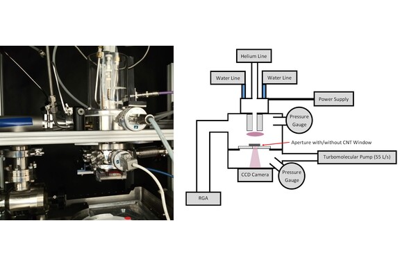
Hollow cathode plasmas are common extreme ultraviolet (EUV) lamps used for material characterization. However, the relatively high pressure of the plasma can affect downstream instruments, as well as absorb the EUV. EUV windows are difficult to fabricate due to EUV’s strong interaction with all materials. We present a carbon nanotube (CNT) microfabricated window composed of multiple high aspect-ratio columns in parallel. The open areas allow wide bandpass transmission, while the walls restrict gas flow. We model the CNT window transmission as a weight function on the light from of a Mcpherson 629-like hollow cathode helium plasma in visible wavelengths. We model the CNT window differential pumping as a series of columns between two chambers of different pressures.

Traditional collimators typically require large optics and/or long pathlengths which makes miniaturization difficult. Carbon nanotube templated microfabrication offers a solution to pattern small 3D structures, such as parallel hole collimators. Here we present the characterization of a carbon nanotube parallel hole collimator design and its efficacy in visible and short wavelength infrared light. Comparison to geometric and far field diffraction models are shown to give a close fit, making this a promising technology for miniaturized diffuse light collimation.

Some of the least reflective materials are vertically aligned carbon nanotubes (VACNTs). However, VACNT films are extremely fragile, restricting the range of applications where they can be used. Here, we have formed VACNT/carbon composite films with greater than 500× stiffness and 50× strength compared to as-grown VACNTs while maintaining ultralow reflectance. This is achieved using an infiltration process that coats the individual nanotubes with a thin layer of nanocrystalline carbon, locking the nanotubes together, and then adding lateral subwavelength surface topography to the tops of the VACNTs with an oxygen plasma etch to reduce the reflectance. While still a delicate material, these composites are robust enough to be exposed to water and handled. We demonstrated that these composites can be transferred from the growth substrate to other surfaces resulting in a reflectance of less than 0.1%.acs

DNA origami-assembled metal–semiconductor junctions have been formed as a step toward application of these nanomaterials in nanoelectronics. Previously, techniques such as electroless plating, electrochemical deposition, or photochemical reduction have been used to connect metal and semiconductor nanomaterials into desired patterns on DNA templates. To improve over prior work and provide a more general framework for the creation of electronic nanodevices as an alternative nanofabrication step, we have developed a method to connect gold (Au) and tellurium (Te) nanorods on a single DNA origami template without electroplating by annealing after coating with a heat-resistant polymer. Bar DNA origami templates (17 nm × 410 nm) were seeded site-specifically with Au and Te nanorods in an alternating manner. These templates were then coated with a polymer and annealed at different temperatures. At 170 °C, the Au and Te nanorods were best connected, and we hypothesize that the junctions were established primarily due to the atomic mobility of gold. Electrical characterization of these Au/Te/Au assemblies revealed some nonlinear current–voltage curves, as well as linear plots that are explained. This annealing method and the metal–semiconductor nanomaterials that are formed simply through controlled seeding and annealing on DNA origami templates have potential to yield complex nanoelectronic devices in the future.

Several electrical devices are formed by growing vertically aligned carbon nanotube (CNT) structures directly on a substrate. In order to attain high aspect ratio CNT forest growths, a support layer for the CNT catalyst, usually alumina, is generally required. In many cases, it has been found that current can pass from a conductive substrate, across the alumina support layer, and through the CNTs with minimal resistance. This is surprising in the cases where alumina is used because alumina has a resistivity of 𝜌>1014ρ>1014 Ω cm. This paper explores the mechanism responsible for current being able to cross the alumina support layer with minimal resistance following CNT growth by using scanning transmission electron microscopy imaging, energy dispersive x-ray spectroscopy, secondary ion mass spectroscopy, and two-point current-voltage (I-V) measurements. Through these methods, it is determined that exposure to the carbonaceous gas used during the CNT growth process is primarily responsible for this phenomenon.