Selected Publications
Qi Wang and D. D. Allred (et al.)
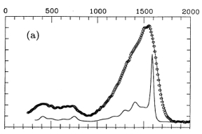
In the first-order Raman spectrum of amorphous carbon (a-C) there is a low-frequency feature in the 200-900-cm-1 region. This feature is characteristic of the highly disordered amorphous-carbon materials. We note that the intensity of this feature is very sensitive to the thermal history of samples, thus suggesting that it is an important measure of the degree of disorder of the a-C materials. We also discuss the relationship between this feature and the phonon density of states of graphite.
F. Yuan, Y. Shi, L. V. Knight, R. T. Perkins, and D. D. Allred
We are studying the possibility of producing precision, aspherical mirrors for X-rays and visible light. Our study examines the use of ultrastructure processing to replace mechanical methods of material removal. The method starts with a chemically-mechanically polished, flat silicon wafer. The aim is to preserve atomic scale smoothness of the surface wafer while the wafer is bent to a desired figure. We report measurements of the mechanical properties of various stressing layers. This involves measuring the deformation of several thin silicon wafers coated with chemically vapor deposited nickel and boron films of known thickness. We have found that, under normal conditions, the film does not add to the microroughness of the substrate on either the front or the back surfaces. Film and substrate thicknesses, however, vary by as much as 10%. This is the present limit on figure accuracy. We have developed a model that describes bending of B/Si and Ni/Si structures. The model relates stress and Young's modulus to the measured thickness of the film, and the thickness and curvature of the substrate. This approach is used to measure the stress and Young's modulus for boron and nickel films. The Young's modulus E(f) was 3.05 x 10(12) Pa for the boron films and 1.4 x 10(10) Pa for the nickel films. From the relationship developed and verified for predicting the radii of curvature of the substrate, it may be possible to define a film thickness pattern which would provide a desired optical figure.
David D. Allred, Ming Cai, Qi Wang, and Dorian M. Hatch (et al.)
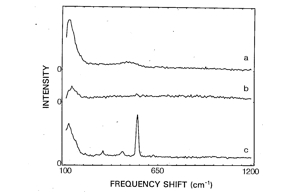
Raman spectra are reported from MoSi2 polycrystalline powder and soft x-ray Mo/Si multilayers. The sharp lines at 323 and 438 cm−1 are all due to crystalline MoSi2. These lines in the powder sample intensify with annealing. The Raman spectra of as-deposited multilayers shows a broad asymmetric peak, highest at about 480 cm−1. We attribute this to α-Si which is highly disordered. In contrast to α-Si in semiconductor/semiconductor and semiconductor/dielectric multilayers, in the Mo/Si samples the Raman signal can vanish after modest heating. This provides evidence that the composition of the silicon component of the multilayer changes even with 200°C annealing. Further annealing also produces the signature for crystalline MoSi2 in the multilayer samples. This is the first report of the characterization of Mo/Si soft x-ray multilayers by Raman spectroscopy, and it indicates that Raman spectroscopy may be an effective technique for characterizing these soft x-ray multilayers and may be useful in studying their interfaces.
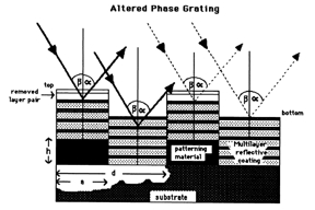
X-ray phase diffraction gratings can be designed to behave in a fashion similar to blazed gratings, directing the majority of the energy into certain desired orders. They should be easy to fabricate using conventional semiconductor production technology, and offer advantages in design flexibility and efficiency over conventional amplitude grating or blazed grating structures. As a multilayered structure, a phase grating has structure in depth as well as across the surface. Most theoretical analyses in the literature treat the embedded structure through simplifying approximations or assumptions. We will discuss a model which treats the embedded structure explicitly using the Fresnel-Kirchhoff integral in the Fraunhofer diffraction limit. This approach produces a set of equations which are identical to the result for an amplitude diffraction grating except for an additional factor which depends on the phase relationships of the various surfaces in the multilayer stack.
Wael I. Karain, Larry V. Knight, and David D. Allred (et al.)
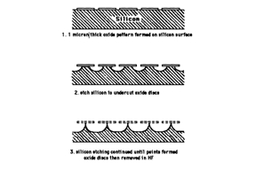
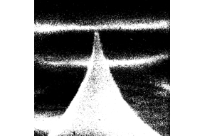
We have produced arrays of 10,000 sharp p-type silicon points using an etch plus oxidation method. These points were used as electron emitters. No high vacuum caseation or high temperature cleaning was needed to observe the electron emission. These are seen to be photosensitive sources of electrons at 200 K and 300 K. They were also used to produce AlK(alpha ) x rays. This constitutes the first use of etched, point arrays for generating electrons for x-ray sources.
W. I. Karain, Larry V. Knight, and David D. Allred (et al.)