Selected Publications
Basu Ram Aryal, Tyler Westover, Dulashani R. Ranasinghe, DIana Gabriela Calvopiña, Bibek Uprety, John N. Harb, Robert C. Davis, and Adam T. Woolley
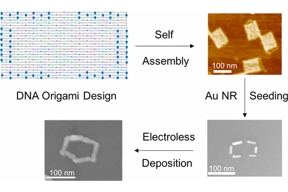
Bottom-up nanofabrication is increasingly making use of self-assembled DNA to fabricate nanowires and potential integrated circuits, although yields of such electronic nanostructures are inadequate, as is the ability to reliably make electrical measurements on them. In this paper, we report improved yields and unprecedented conductivity measurements for Au nanowires created on DNA origami tile substrates. We created several different self-assembled Au nanowire arrangements on DNA origami tiles that are approximately 70 nm x 90 nm, through anisotropic growth of Au nanorods attached to specific sites. Modifications to the tile design increased yields of the final desired nanostructures as much as six fold. In addition, we measured the conductivity of Au nanowires created on these DNA tiles (~130 nm long, 10 nm diameter and 40 nm spacing between measurement points) with a four-point measurement technique that utilized electron beam induced metal deposition to form probe electrodes. These nanowires formed on single DNA origami tiles were electrically conductive, having having resistivities as low as 4.24 x 10⁻⁵ Ω m. . This work demonstrates the creation and measurement of inorganic nanowires on single DNA origami tiles as a promising path toward future bottom-up fabrication of nanoelectronics.

Guohai Chen, Berg Dodson, Robert C. Davis, and Richard R. Vanfleet (et al.)
Test disk electrodes were fabricated from carbon nanotubes (CNT) using the Carbon Nanotube Templated Microfabrication (CNT-M) technique. The CNT-M process uses patterned growth of carbon nanotube forests from surfaces to form complex patterns, enabling electrode sizing and shaping. The additional carbon infiltration process stabilizes these structures for further processing and handling. At a macroscopic scale, the electrochemical, electrical and magnetic properties, and magnetic resonance imaging (MRI) characteristics of the disk electrodes were investigated; their microstructure was also assessed. CNT disk electrodes showed electrical resistivity around 1 Ω·cm, charge storage capacity between 3.4 and 38.4 mC/cm2, low electrochemical impedance and magnetic susceptibility of −5.9 to −8.1 ppm, closely matched to that of tissue (∼−9 ppm). Phantom MR imaging experiments showed almost no distortion caused by these electrodes compared with Cu and Pt-Ir reference electrodes, indicating the potential for significant improvement in accurate tip visualization.
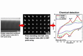
Guohai Chen, Berg Dodson, David M. Hedges, Scott C. Steffensen, John N. Harb, Richard Vanfleet, and Robert Davis (et al.)
Microelectrode arrays of carbon nanotube (CNT)/carbon composite posts with high aspect ratio and millimeter-length were fabricated using carbon-nanotube-templated microfabrication with a sacrificial “hedge”. The high aspect ratio, mechanical robustness, and electrical conductivity of these electrodes make them a potential candidate for next-generation neural interfacing. Electrochemical measurements were also demonstrated using an individual CNT post microelectrode with a diameter of 25 μm and a length of 1 mm to perform cyclic voltammetry on both methyl viologen and dopamine in a phosphate-buffered saline solution. In addition to detection of the characteristic peaks, the CNT post microelectrodes show a fast electrochemical response, which may be enabling for in vivo and/or in vitro measurements. The CNT post electrode fabrication process was also integrated with other microfabrication techniques, resulting in individually addressable electrodes.
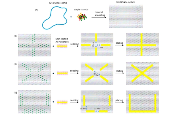
Bibek Uprety, John Jensen, Basu R. Aryal, Robert C. Davis, Adam T. Woolley, and John N. Harb
This work examines the anisotropic electroless plating of DNA-functionalized gold nanorods attached to a DNA origami template to fabricate continuous metal structures of rectanglar, square, and T shapes. DNA origami, a versatile method for assembling a variety of 2- and 3-D nanostructures, is utilized to construct the DNA breadboard template used for this study. Staple strands on selective sites of the breadboard template are extended with an additional nucleotide sequence for the attachment of DNA-functionalized gold nanorods to the template via base pairing. The nanorod-seeded DNA templates are then introduced into an electroless gold plating solution to determine the extent to which the anisotropic growth of the nanorods is able to fill the gaps between seeds to create continuous structures. Our results show that the DNA-functionalized nanorods grow anisotropically during plating at a rate that is approximately 4 times faster in the length direction than in the width direction to effectively fill gaps of up to 11–13 nm in length. The feasibility of using this directional growth at specific sites to enable the fabrication of continuous metal nanostructures with diameters as thin as 10 nm is demonstrated and represents important progress toward the creation of devices and systems based on self-assembled biological templates.
Lawrence K. Barrett, Juichin Fan, Kevin Laughlin, Sterling Baird, John N. Harb, Richard R. Vanfleet, and Robert C. Davis
A nanoporous carbon monolith structure has been developed for use as a scaffold for silicon anodes for lithium batteries. This scaffold was fabricated by coating vertically aligned carbon nanotubes in a highly conformal coating of nanocrystalline carbon, applied via atmospheric pressure chemical vapor deposition. The coating increases the mechanical stability of the nanotube structure, which provides electrically conductive pathways through the anode. Silicon anodes were fabricated with the monoliths by low pressure chemical vapor infiltration of silicon. This platform allows the carbon and silicon volume fractions to be independently varied in the anode. Anodes with a low silicon content (less than 5% by volume) showed high stability in cycling against lithium with a capacity retention of 89.7% between cycles 2 and 185. Anodes with a high silicon content (∼25% by volume) showed poor capacity retention when the carbon content was low (<40% by volume), and transmission electron microscopy analysis indicated that the anodes failed due to the destruction of the nanocrystalline carbon coating during cycling. However, by increasing the carbon content to ∼60% volume percent in the monolith, capacity retention was substantially stabilized even for anodes with very high silicon loadings. These stabilized electrodes exhibited volumetric capacities as high as ∼1000 mA h/ml and retained over 725 mA h/ml by cycle 100.
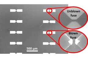
Kevin R. Laughlin, Sarah Jamieson, Anthony C. Pearson, Hao Wang, Richard R. Vanfleet, Robert C. Davis, Matthew R. Linford, and Barry M. Lunt
In this study, we have fabricated nanofuses from thin-film, arc-deposited carbon for use in permanent data storage. Thin-film carbon fuses have fewer fabrication barriers and retain the required resistivity and structural stability to act as a data-storage medium. Carbon thin films were characterized for their electrical, microstructural, and chemical bonding properties. Annealing these films in an argon environment at 400 °C reduced the resistivity from about 4 × 10⁻² Ω cm as deposited to about 5 × 10⁻⁴ Ω cm, allowing a lower blowing voltage. Nanofuses with widths ranging from 200 to 60 nm were fabricated and tested. They blow with voltages between 2 and 5.5 V, and the nanofuses remain stable in both “1” and “0” states under a constantly applied read voltage of 1 V for over 90 h.